 Paper →
Overview
As a DOE Graduate Research Internship Program (GRIP) intern with the OASIS group at Brookhaven National Laboratory, working within the Co-Design Center for Quantum Advantage (C2QA), I designed, built, and commissioned a custom DC magnetron reactive sputtering system to grow zirconium nitride (ZrN) thin films. ZrN is an appealing alternative base-layer material for superconducting qubits: it is CMOS-compatible, forms a chemically stable surface, and has reported superconducting transition temperatures of several kelvin — all properties relevant to reducing the two-level-system defects that currently limit qubit coherence times.
Rather than sputtering from an expensive, long-lead-time pre-formed ZrN target, I grew films by reactively sputtering an elemental zirconium target in an Ar/N₂ gas mixture, letting the nitride phase form in situ. Over the course of the project I performed 17 thin-film deposition runs on Si and MgO substrates, varying gas ratio, pressure, substrate temperature, and cooldown environment, then characterized each film's electrical transport from room temperature down to 3–4 K.
The Sputtering System
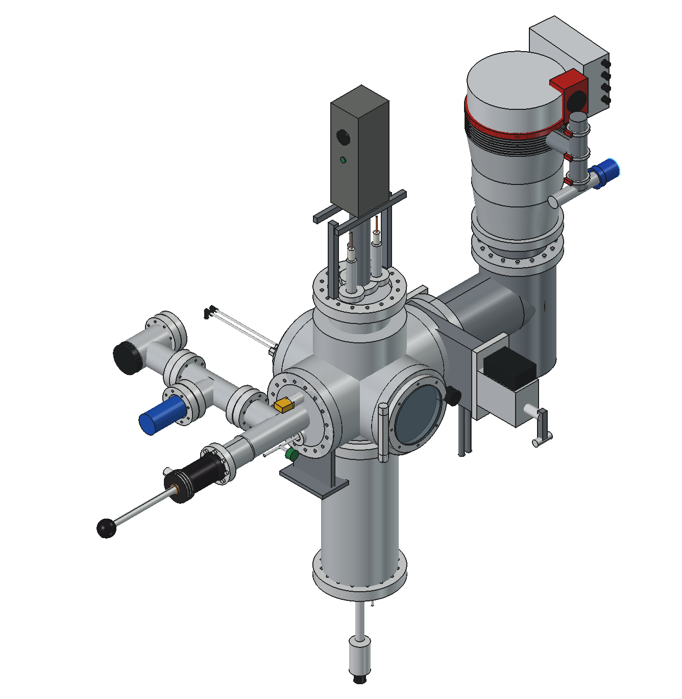
Above is a 3D model of the custom DC magnetron reactive sputtering system I designed for this project, shown in its full CAD assembly — the main four-way vacuum chamber, turbo pump stack, gate valve, ion gauge, RGA, and linear feedthrough.
What I Did
This project spanned the full pipeline from hardware to data analysis:
• Designed and assembled a four-subsystem DC magnetron sputtering system (vacuum, deposition/plasma, gas
delivery, and thermal management) from the ground up.
• Developed and executed a 17-run deposition series on Si and MgO substrates, systematically varying
Ar:N₂ flow ratio, working pressure, substrate temperature (up to 800 °C), and cooldown atmosphere.
• Calibrated film thickness using AFM step-height measurements against a lithographically defined edge to
correct in-situ QCM readings.
• Wire-bonded films in a four-terminal (Kelvin) configuration and measured temperature-dependent
resistance, R(T), in a cryostat from ~300 K to ~3–4 K.
• Analyzed residual-resistance ratios (RRR) across the deposition series to quantify metallic versus
nonmetallic transport and identify the growth parameters driving the difference.
What I Found
The deposition series produced a wide range of transport behavior, from strongly nonmetallic to metallic, showing just how sensitive ZrN film properties are to growth conditions. Heating alone didn't reliably improve transport — some heated films on Si actually became more resistive at low temperature — but switching the post-deposition cooldown atmosphere from vacuum to flowing N₂ recovered metallic behavior, pointing to stoichiometry and post-growth environment as key levers. The best film of the series, grown on MgO at 800 °C, reached the highest residual-resistance ratio obtained (RRR = 1.293). No film showed a clear superconducting transition above the experimental base temperature, which — combined with what's known about disorder suppressing Tc in ZrN — points to structural and compositional characterization (XRD, XPS) as the necessary next step.
This project gave me an end-to-end view of experimental quantum materials research: building the hardware, running a systematic growth study, and turning noisy transport data into a physically grounded story about what's limiting a candidate qubit material. It's directly shaped how I think about the link between materials science and quantum hardware performance, and reinforced my interest in contributing to quantum computing hardware research going forward.